

Neutron Depth Profiling (NDP) Studies at the Penn State University Nuclear Reactor Reactor
| Participants: | K. Ünlü , Professor of Mechanical and Nuclear Engineering |
| S. Çetiner, Grad. Student | |
| J. Hoover, Undergrad. Student | |
| Services Provided: | Neutron Beam Laboratory |
| Sponsor: | Department of Energy, under Nuclear Energy Engineering Research (NEER) grant |
Introduction
Neutron Depth Profiling (NDP) is a near-surface-analysis technique to measure the spatial distribution of certain isotopes of technological importance in any substrate. The NDP technique was originally developed by Ziegler et al [ 1 ] in 1972, and later thoroughly investigated by Biersack et al. [ 2 , 3 ] The basis of NDP is the irradiation of a sample with thermal or sub-thermal neutrons and the subsequent release of charged particles due to neutron induced exoergic charged particle reactions. Neutrons interact with the nuclei of isotopes 10 B, 3 He, 6 Li, 7 Be and 22 Na etc, and release mono energetic charged particles, e.g. alpha particles or protons, and recoil atoms. Figure 1 is an illustration of this reaction for 10 B, and Table 1 gives a detailed listing of other relevant NDP reactions.
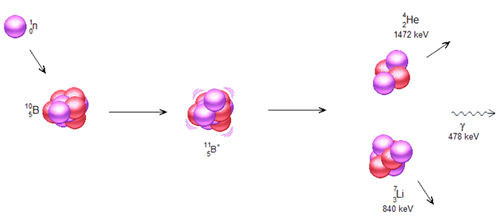
Figure 1 . Neutron-boron reaction that creates charged particles, 7 Li and 4 He.
The charged particles travel outward and lose energy by numerous interactions with the electrons of the host matrix. Measuring the residual energy of the charged particles or recoil atoms and knowing the stopping power of the host matrix allow for the determination of the depth profile of the isotope of interest inside the matrix. The reader is recommended to refer K. Ünlü et al [ 4 ] for a comprehensive discussion.
Figure 2 presents an example to the correlation between the range and the initial energy of alpha particles in silicon. The dotted red lines indicate the energy of alpha particles coming out of the 10 B (n, a) 7 Li reaction: Vertical line is the initial energy, which is 1472 keV and the horizontal line is the range of alpha particles in elemental silicon. What this tells us is that alpha particles that are from 10 B (n, a) 7 Li reaction travel 5 µm on the average within the silicon matrix until they ultimately come to a full stop.
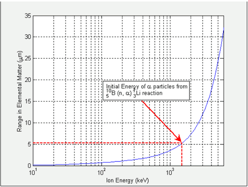
Figure 2 . The plot gives an example to the mapping between the energy and the theoretical range of alpha particles in silicon. The data is generated by SRIM 2003 software made available by Ziegler et.al.
Principles of NDP
Figure 4 shows the schematic of a conventional NDP setup and Figure 3 shows the block diagram of a conventional NDP setup. The detector used in NDP setup is operated in vacuum (around 10 -6 torr) to eliminate alpha particle attenuation while they travel from the sample to the detector surface. Figure 5 shows the picture of the vacuum chamber that encloses the sample and the detector, and the electronics. During the experiment, neutrons enter the chamber through thin Al windows. Neutrons hit the sample and interact with 10 B isotopes creating charged particles, alpha and 7 Li. Then some of the charged particles move towards the detector and hit the detector surface resulting in a small charge signal. This signal is then sent to the preamplifier where it is amplified and converted into a voltage signal. After that it is amplified again in the amplifier. The analog signal is then converted into a digital signal in an ADC unit (Analog-to-Digital Converter) and the digital signal is displayed on the computer. The instrumentation can also be seen in Figure 5 next to the vacuum chamber.
Table 1 . Useful NDP reactions
|
|---|

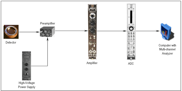
Figure 3 . The block diagram of the conventional NDP setup.
NDP Techniques
There are two ways to correlate the measured energy of the particle to the depth the particle is created: by directly measuring the particle energy through pulse-height analysis, or by measuring the intervals between the time that charged particles are created and the time they hit the surface of the detector through time base analysis.
The first technique will be referred to as Conventional NDP , and the latter as Time-of-Flight NDP (TOF-NDP) throughout this text.
In the conventional NDP, one directly measures the particle energy. Once the energy spectrum is taken, using the stopping power correlations pertinent to the material of interest, each energy bin in the spectrum is matched to the corresponding depth of isotope of interest that underwent the charged particle reaction. The energy difference from the initial particle energy is an indication of how far these particles traveled within the matrix; in other words, how deep the isotope of interest reside. Figure 3 and Figure 4 illustrate the experimental setup for the conventional NDP.
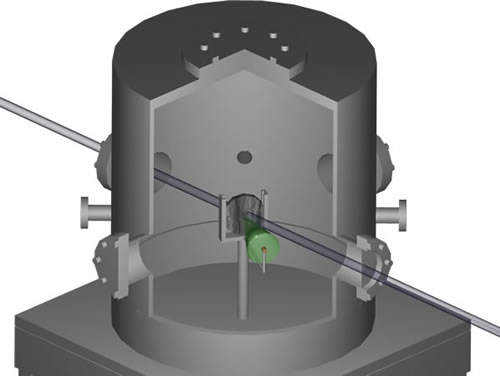
Figure 4 . The schematic of the conventional NDP experimental setup
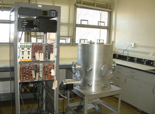
Figure 5 . NDP setup at Breazeale Nuclear Reactor: electronic instrumentation panel (left) and the vacuum chamber (right)
Time-Of-Flight technique does not directly measure particle energy. Rather than measuring energy, one can measure the time intervals between the time that the charged particles are created and the time they hit the surface of the detector. In order to do that, one needs two separate detectors: one for the start signal that is created by prompt electrons, which are theoretically instantly created when a charged particle reaction takes place, and another for stop signal created by charged particles or recoil nuclei. The time difference between the two signals gives a measure of how fast particle traverses, in other words how energetic it is, with the well-known formula:
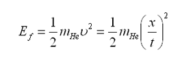
where ![]() is the energy of alpha particles when they leave the sample,
is the energy of alpha particles when they leave the sample, ![]() is the distance of the detector to the sample, and
is the distance of the detector to the sample, and ![]() is the time interval between the alpha particles are created and they hit the detector surface.
is the time interval between the alpha particles are created and they hit the detector surface.
Time-Of-Flight NDP block diagram is given in Figure 6 .

Figure 6 . Block diagram of Time-of-Flight NDP setup
Applications of NDP
The NDP technique has diverse applications in microelectronics, optical signal processing, surface modification technologies, and new technology alloy development.
These applications involve the measurement of the behavior of the light elements such as helium, boron, lithium, beryllium, etc. in various materials. The majority of these applications involve boron depth profiling in semiconductor materials. Two of the most common applications of NDP are briefly described below.
1. 3 He in alloys
The radiation damage in alloys due to 3 He implantation is an important issue that can be investigated by using the NDP technique. Helium can modify material properties because, when introduced into materials, it tends to nucleate as small gas clusters in lattice defects. If helium fluence is increased the small gas clusters combine and form gas bubbles. Gas bubbles may recombine and create a pressurized cavity beneath the material surface. When the pressure of the cavity is high enough, it can form blisters. Rupturing of these blisters causes surface flaking or exfoliation.
Pressurized helium gas bubbles inside materials may also cause cracks. Formation of cracks and propagation of cracks to the bulk can ultimately compromise the structural integrity of materials. The shape of the depth profile gives information about possible microstructural changes that occur in an alloy. For example, the differences in spatial distribution of implanted Helium in a near-surface region and across interfacial boundaries can significantly affect the Helium release phenomenon.
When a thermal neutron strikes the sample with 3 He, the 3 He (n, p) 3 H reaction takes place. From the proton energy spectrum, one can determine the 3 He distribution within the sample. The energy spectrum can be converted to depth profile using the stopping power correlations and corresponding counts are translated to isotopic concentration profile. K. Ünlü et al [ 5 ] gives a more detailed explanation on 3 He analysis in alloys.
2. 10 B in Microelectronics Materials
The application of NDP in microelectronics has been an important topic due to the extensive use of boron in semiconductor device fabrication. Some of the important applications for semiconductor industry are:
• Study of boron distributions in semiconductor materials as a function of wafer treatment.
• Investigation of boron transport in semiconductor materials, especially across oxide surfaces.
• Study of boron concentration in microelectronics passive layers as it affects melting temperatures.
• Study of boron doses of semiconductor materials for dose calibration of commercial ion implant systems.
Please refer to K. Ünlü et al [ 6 ] for further discussion on this issue.
Experiments Performed at Penn State Breazeale Nuclear Reactor
1. Conventional NDP Experiments with Intel Borophosphosilicate Glass Sample
Borophosphosilicate glass (BPSG) is used as an insulating layer on high-density integrated circuits. The thickness of the boron layer in BPSG is an important factor in the production of multilayer circuits. A more detailed discussion can be found in K. Ünlü , et al [ 7 ] .
Figure 7 illustrates the results of an NDP experiment performed with an Intel Borophosphosilicate glass wafer. The energy spectrum of the alpha peak plotted in the top figure is converted into the atomic concentration versus isotope depth from the surface of the matrix. Note that the measured particle energy the horizontal axis in the top figure- carries information about the distance alpha particles traveled in the matrix before they hit the surface of the detector, i.e. the more energy they have the closer they are to the surface.
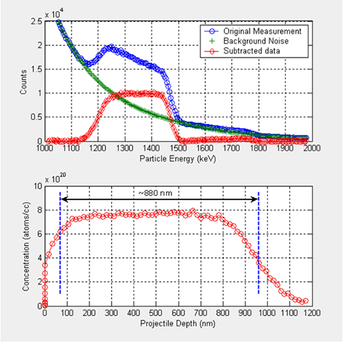
Figure 7 . Experimental data for Intel Borophosphosilicate glass wafer (top), and concentration vs. projectile depth (bottom).
At the top figure, blue plot represents the original measurement for the alpha peak during the experiment. As can be seen, the original measurement has significant noise content in it. The background noise can be fitted to a polynomial, as presented with the green data. If this content is subtracted from the measurement, one obtains the net spectrum as plotted in red at the top figure.
The bottom figure is obtained by using the net spectrum in the NDP calculations. As we discussed earlier, particle energy is translated to isotope depth and net count into isotope concentration in the calculations.
The origin of the horizontal axis corresponds to the surface of the wafer. The distribution tends to disperse around the edges because of the diffusion mechanism, predominantly into the silicon wafer. The figure also illustrates an interpretation of the thickness of the Borophosphosilicate glass layer.
The resolution of the current measurement system for this sample is about 30 nm.
2. Conventional NDP Experiments with AMD 10 B Implanted Silicon Wafer
Ion implantation is the most frequent and widely practiced method of doping silicon during semiconductor device fabrication. The typical fabrication plant has a series of ion implanters set up to introduce a dopant like boron. The dose of these dopants need to be within a limited tolerance and desired distribution profile in order for reliable device performance. Another important issue is that these multiple implanters must provide the same dose/profile over a period of time in order to yield consistent products. The accurate characterization of the implanted dose is therefore very important.
Figure 8 shows the results of an NDP experiment for a 120 keV 10 B implanted AMD silicon wafer at a total dose of 2.0 × 10 16 atoms/cm 2 . As with the Borophosphosilicate glass wafer, energy spectrum is converted into isotope depth, and the number of counts into 10 B concentration in the matrix.
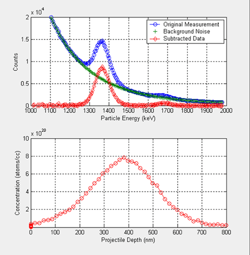
Figure 8 . Experimental measurements with AMD wafer (top), and concentration profile vs. projectile depth (bottom).
The background noise removal is achieved with the same procedure explained for the Borophosphosilicate glass wafer. In a profile of an implanted isotope, one expects a Gaussian-like distribution as shown at the bottom figure. The slight skewness or asymmetry of the peak is an artifact of the nonlinearity of the scattering process in terms of energy within solids.
Projections on NDP Experiments
Our group already reproduced the conventional NDP experiments performed at University of Texas at Austin and Cornell University before, as presented in Figure 7 and Figure 8 . We are working on replicating the same experiments, among others, with the TOF-NDP technique. TOF-NDP at Penn State University is continuing to develop. Figure 9 shows the detailed schematics of the latest NDP setup. We expect that TOF NDP will provide up to a ten times better resolution than the conventional NDP, which will make the depth vs. concentration measurements of ultra shallow junction devices possible. We think that this improvement will have a significant contribution to silicon industry as the dimension of micro devices gets miniaturized every day.

Figure 9 . Time-Of-Flight NDP schematics
Acknowledgement
This project is sponsored by U.S. Department of Energy under Nuclear Energy Engineering Research (NEER) grant.
References
• J.F. Ziegler, G.W. Cole, and J.E.E. Baglin, J. Appl. Phys. , Vol. 43 (1972) 3809.
• K. Ünlü and B.W. Wehring, Nucl. Instr. And Meth. Phys. Res. A , 353, (1994) 402.
• K. Ünlü et al., IEEE Proc. 11 th Int. Conf. on Ion Imp. Tech., Vol. 1, 1996, p 575.